SINCHON·INT′l
SINCHON·INT′l
- MIRAE

show mobile menu
mobile menu
Next-Gen Sensors: Exploring the Promises and Potential of Metal Oxide Phototransistors
A review on the recent developments in metal oxide phototransistors indicates improvements made to the photodetection range
Research published online in Advanced Materials in May, 2021
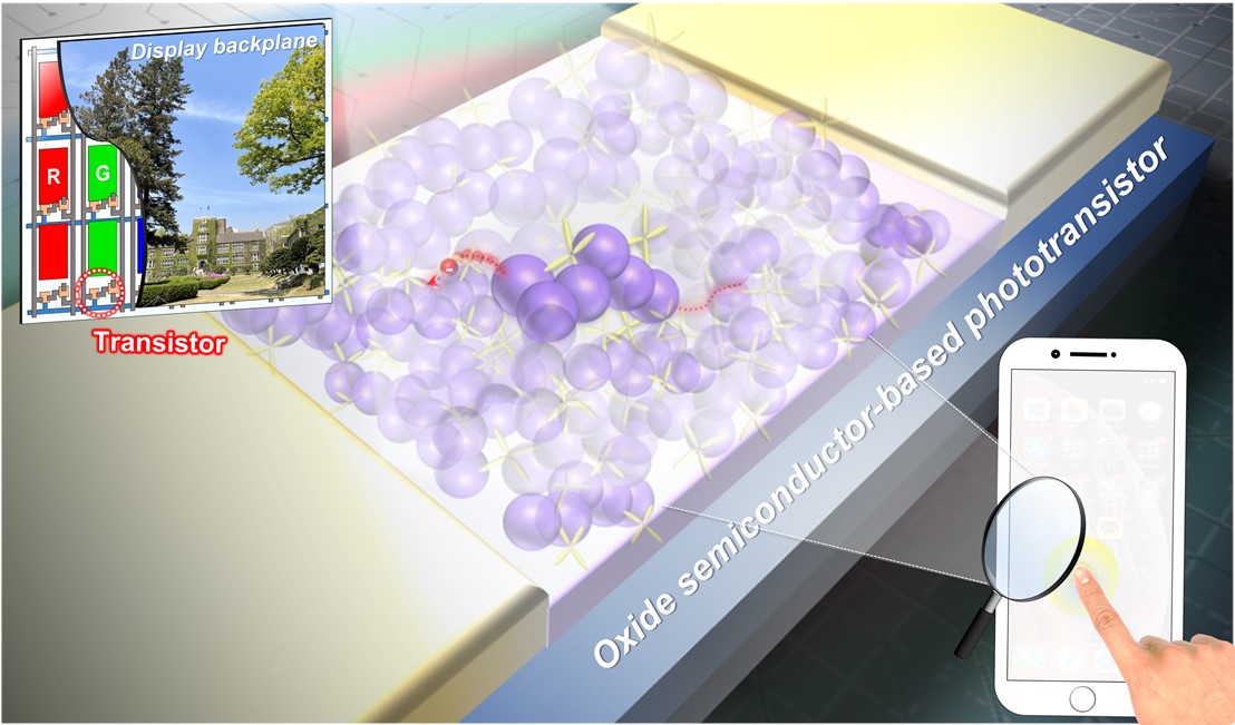
Transistors have ushered in the semiconductor era, and recently developed phototransistors are at the core of the 4th generation IoT sensors
Photo courtesy: Hyun Jae Kim from Yonsei University
The invention of the transistor in 1947 allowed developing reliable, smaller, and more energy efficient electronic devices. Invention of the transistor, the building block of electronics, heralded the electronic age, and marked remarkable progress in the field of electronics in general. One such milestone was the commercialization of metal oxide-based thin-film transistors (TFTs) in 2012. These oxide semiconductor-based TFTs find wide application in liquid crystal displays (LCDs) and organic light-emitting diode (OLED) displays. In addition, research is ongoing to find new applications of metal oxide semiconductors beyond that in displays, such as memory and sensor applications.
In recent years, photosensors, which generate a current when struck with light, have attracted attention owing to their vast applicability. Out of the different types of photosensors, phototransistors have a similar structure to TFTs; of late, interest in using oxide TFTs as phototransistors is increasing.
Given the importance of phototransistors, researchers from Korea, including Prof. Hyun Jae Kim from Yonsei University, have tracked the progress made in oxide semiconductor and have consolidated their findings in a review article published in Advanced Materials. They hope their article will provide insights into the development of metal oxide phototransistors and be a good reference material for those interested in the field.
The main limitations of oxide phototransistor are related to the large energy bandgap and the oxygen-related defects of the semiconductor. The large energy bandgap prevents the phototransistor from absorbing light of longer wavelengths, limiting its photodetection range to the ultraviolet region, while the oxygen-related defects cause persistent photocurrents (PPC) that lower its stability.
In their article, the researchers also highlight research from the last decade aimed at combating these limitations of phototransistors. Engineering the oxide semiconductor layer seems to be the most popular technique to improve the performance of phototransistors. Techniques like surface treatment and doping the oxide layer are being developed to reduce defects and increase the photodetection range. Another technique involves utilizing additional oxide layers for light absorption, which lowers the energy bandgap and allows the fabrication of multi-oxide layer phototransistors.
Other studies suggest using non-oxide materials, such as chalcogenides, organics, perovskites, and nanodot materials like nanoparticles of gold, silver, and platinum, in combination with the oxide semiconducting layer to create hybrid structures that improve the performance and photodetection range of phototransistors.
In summary, existing research on metal oxide phototransistors mostly focuses on improving the photodetection range and PPC phenomenon.
The researchers are optimistic about the potential of oxide phototransistors. However, they acknowledge the need for further progress. "Although studies have improved light detection in the visible light region, research is still limited on infrared detection with metal oxide phototransistors. More advanced methods are needed to improve the PPC phenomenon." concludes Prof. Kim.
Recommended Articles
Professor Jong-Hyun Ahn
Novel technique for producing high-resolution micro-LED displays

Professor Seong Chan Jun

Professor Donghyun Kim
Array of hope: Up close and personal with mitochondria in neurons


