SINCHON·INT′l
SINCHON·INT′l
- MIRAE

show mobile menu
mobile menu
From 2D layers to 3D structures: Atomically precise fabrication method for nanoelectronics
One of the most notorious features of today’s electronic devices is their incredibly small size, which is now reaching the atomic scale. Advances in nanotechnology and nanomaterials have enabled us to build 2D materials, i.e. sheets of material with a thickness of only one atom. New fabrication methods with 2D materials are actively being researched because, to make useful electronic devices, it is necessary to stack multiple layers of different 2D materials and interconnect them vertically in atomically precise ways.
In traditional printed circuit boards, vias, which are akin to small vertical metal-covered tunnels, create electrical contacts across the layers to interconnect them vertically as desired. However, vertically interconnecting stacked layers of 2D materials is harder, and no method was available with the same freedom of design as vias did in traditional printed circuit boards. Moreover, 2D materials exhibit desirable electronic properties when fully encapsulated (sandwiched) between other layers; therefore, a route to access the “buried layers” vertically is required for 2D material-based electronic devices to reach the performance of state-of-the-art electronics.
A team of researchers, including Prof. Gwan-Hyoung Lee from Yonsei University, developed a novel etching method using xenon difluoride gas (XeF2) and 2D graphene (a carbon-based nanomaterial) that can be used to create sophisticated 3D electronic devices out of 2D graphene layers. Etching involves stacking of layers of different materials with pre-defined patterns, followed by attacking with a chemical that eats away at only some of the layers. The idea is to use a pre-patterned layer that is not affected by the chemical as a protective mask (and thus, as a template) such that the underlying layer takes the shape of the mask after the rest has been etched away.
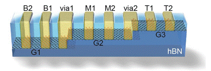 Schematic depicting vertically connected graphene devices through interlayer via. Precisely interconnecting multiple 2D monolayers made of graphene is now possible with a new fabrication method, enabling the development of sophisticated 3D nanoscale electronics matching the performance of state-of-the-art devices.
The new etching method developed takes advantage of the fact that graphene combines with sulfur when exposed to XF2 and becomes fluorographene (FG), which acts as a protective mask for the materials below during the etching process. Additionally, FG forms good electrical contact with metals, which allows for using metals to create the sought-after vias in circuits with multiple graphene layers.
The research team demonstrated that 3D nanometer-scale electronic devices could be made using 2D graphene and this new etching method. These devices had vertical interconnections (vias), giving them important functionalities and allowing the encapsulated graphene layers to be accessed from outside while leaving them protected from outside disturbances. “The outstanding mobility, low contact resistance, and stability obtained from encapsulation make these devices comparable to the state of the art across all metrics,” states Prof. Lee.
What the team achieved is a very important step to further advance in the miniaturization of electronic devices and extend the uses of 2D nanomaterials. “The selective etch process developed is a major capability necessary for the realization of atomically precise, all-2D nanoelectronics as a viable technology,” explains Prof. Lee. Hopefully, the developed method will accelerate the development of nanoscale electronics, so that it finds all sorts of applications to empower us further.
Updated in Dec 2018
Recommended Articles
Professor Jong-Hyun Ahn
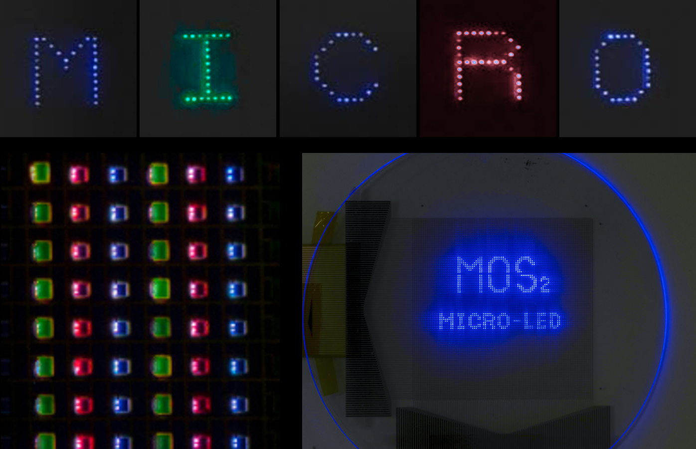
Novel technique for producing high-resolution micro-LED displays

Professor Seong Chan Jun

Professor Donghyun Kim
Array of hope: Up close and personal with mitochondria in neurons


